Hexagonal Boron Nitride (h-BN) on Copper Foil
h-BN on Copper
Product Detail
1. Preparation Method
CVD Method
2. Characterizations
|
|
Monolayer h-BN/hBN |
|
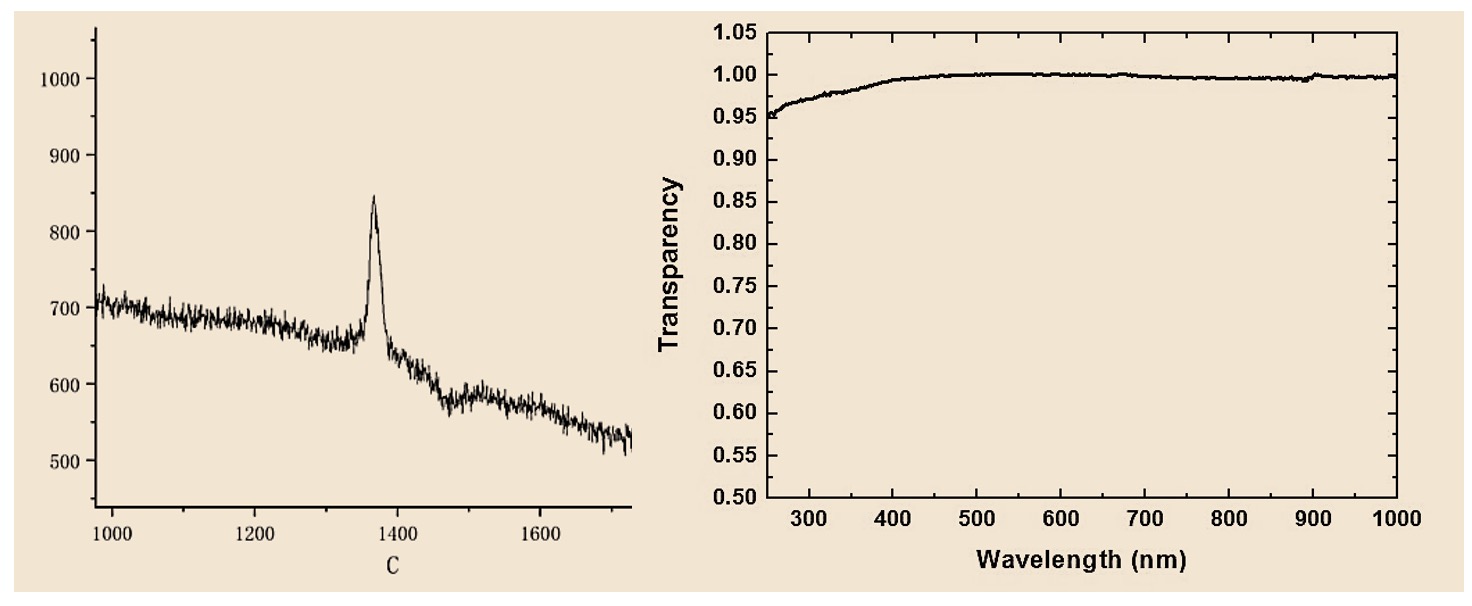
Transparency |
> 97% |
|
hBN Coverage |
100% with sporadic adlayers |
|
Raman Peak |
1370 /cm-1 |
|
Bandgap |
5.97 eV |
|
Grain size |
~100nm |
|
Copper Foil |
25 μm thick |

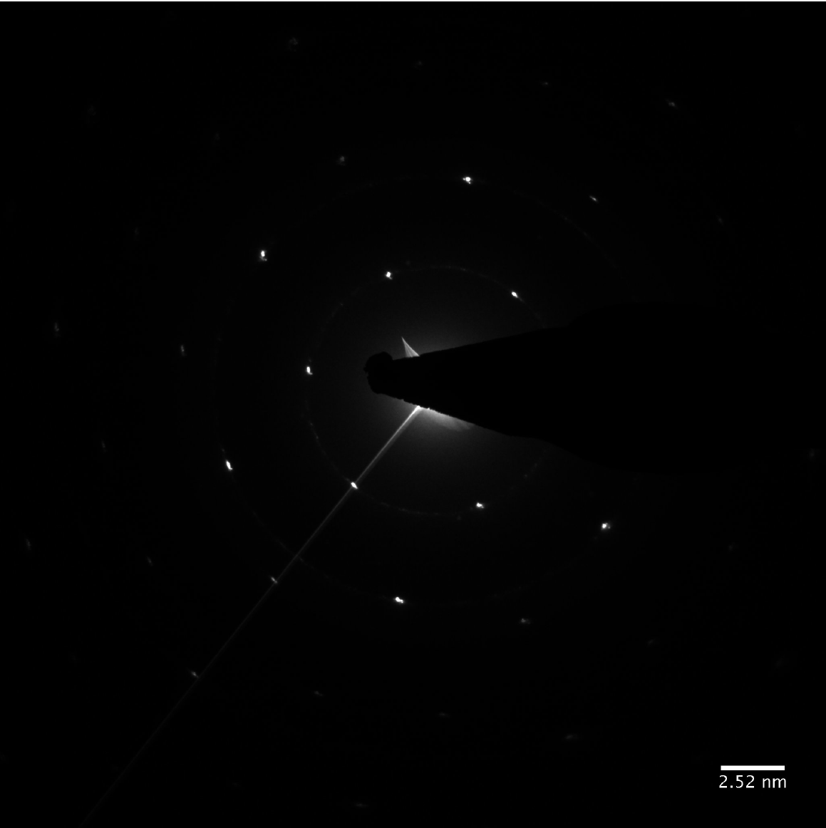
Typical Crystal Diffraction Image of ACS Material Monolayer h-BN

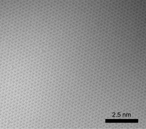
Typical TEM Image of ACS Material Monolayer h-BN

Typical Raman Spectrum of ACS Material Monolayer hBN
* The indicated product metrics are generic to our transfer process. For all ACS Material products, the displayed range represents electronic data that we have obtained using our in-house transfer capabilities to transfer graphene to SiO2. Your own metrics will depend entirely on the transfer methods that you use, and the resultant quality of your transfers.
3. Application Fields
1) Proton conductors
2) Fuel cells
3) Water electrolysis
4) Graphene-based devices
4. User Instruction
1) To ensure the maximum shelf life of your graphene sample, it is best stored under vacuum or in inert atmosphere (Argon or Nitrogen) conditions once the vacuum sealed package has been opened.
2) Products are secured to their underlying plastic containers with four small Kapton tapes, one in each corner. Gently peel the tape or cut off the corners of the foil to release the foil from the plastic container. Please recycle your containers when they are no longer needed.
Disclaimer: ACS Material LLC believes that the information on our website is accurate and represents the best and most current information available to us. ACS Material makes no representations or warranties either express or implied, regarding the suitability of the material for any purpose or the accuracy of the information listed here. Accordingly, ACS Material will not be responsible for damages resulting from use of or reliance upon this information.

