Graphene on Silicon Nitride TEM Grids (2µm holes)
Product Detail
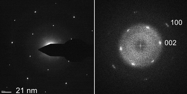
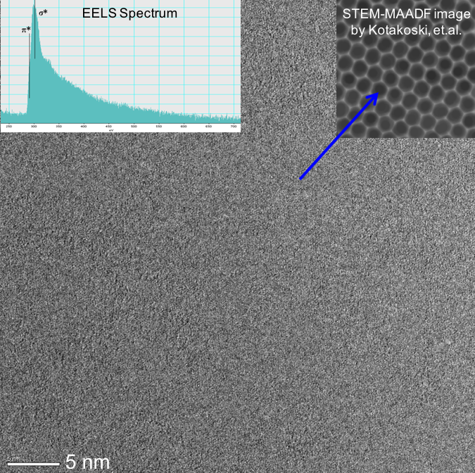
Graphene is proving to be an invaluable tool for TEM imaging. Graphene’s thinness and its superior electrical and thermal conductivity make it an ideal material to use as a support film on TEM grids. Additionally, graphene’s low atomic number minimalizes the scattering of the TEM electron beam, resulting in crisper images.
Continuous graphene films are required for TEM applications. ACS Material has developed a process to deposit high-quality CVD graphene films on silicon nitrate TEM grids using our proprietary trivial transfer method. The TEM substrate features a 3.0mm hexagonal silicon base that is 200µm thick covered with a silicon nitride membrane that’s 200nm thick. The graphene layer is available is 1, 2, 3-5, or 6-8 layers. Roughly 75% of the substrate is covered by graphene. Our TEM grids are free from contamination and facilitate high-contrast TEM images.
Characteristics
Appearance
| Type | Thickness of Graphene | Transparency of Graphene | TEM Grid/AFM Substrate | Support Film |
| 1 Layer | ~0.35nm | ~96.4% | 2μm Hole Silicon Nitride | Silicon Nitride |
| 2 Layers | ~0.7nm | ~92.7% | 2μm Hole Silicon Nitride | Silicon Nitride |
| 3-5 Layers | 1.0-1.7nm | ~85.8-90.4% | 2μm Hole Silicon Nitride | Silicon Nitride |
| 6-8 Layers | 2.1-2.8nm | ~78.5-83.2% | 2μm Hole Silicon Nitride | Silicon Nitride |


