Graphene on Lacey Carbon 300 Mesh Copper TEM Grids
Product Detail
CAS No.: 7782-42-5
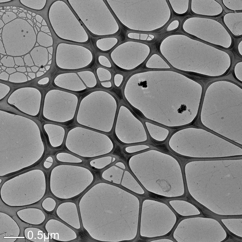
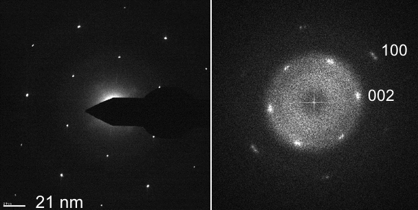
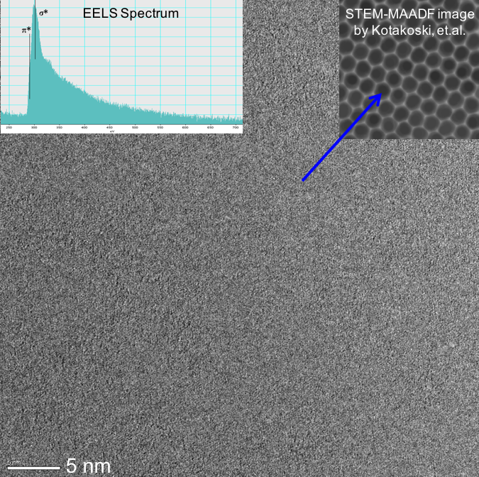
Graphene is proving to be a remarkably versatile material. One of its many uses is transmission electron microscopy (TEM), a powerful imaging technology used by chemical, biological, and physical researchers. TEM captures images of microscopic materials by observing how they interact with an electron beam. The process involves placing the material on a specialized flat surface, or grid, designed to support the material and, at the same time, allow the electron beams to pass through. However, in some cases, the microscopic grid allows super small, nanoscale particles to fall through, making TEM difficult. Suspending a layer of graphene above the grid prevents particles from slipping through without altering the imaging process.
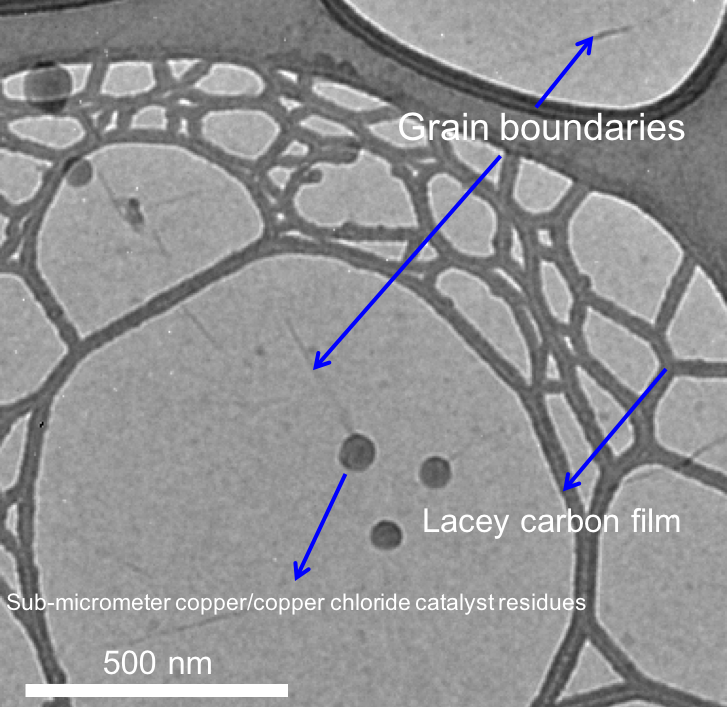
ACS Material offers a selection of TEM support films. Our TEM support films are supported by a lacey carbon film on a 300 mesh copper TEM grid and are created using trivial transfer graphene. Specifications of these advanced TEM grids include:
- Thickness: Our 300 mesh copper TEM grids are available in either 1, 2, 3-5, or 6-8 layer configurations.
- Substrate: The substrate includes a lacey carbon support film on 300 mesh copper TEM grid, featuring a grid hole size of 63 µm.
- Coverage: Graphene coverage of the TEM grid is better than 75%; the graphene coverage is typically >75% of the whole 3.05 mm diameter TEM grid.
- Appearance: The graphene film appears as a near-transparent to light-gray film on the surface of the lacey carbon mesh on a red-brown colored copper TEM grid.
Get the TEM images you need with the help of high-quality graphene-enhanced TEM grids from ACS Material.
- Four thicknesses of CVD graphene: Available in either 1, 2, 3-5 or 6-8 layers
- TEM Substrate: Lacey carbon support film on 300 mesh copper TEM grid (Grid Hole Size: 63µm)
- Graphene coverage of the TEM grid is better than 75%. (The graphene coverage is typically >75% of the whole 3.05mm diameter TEM grid.)
Appearance
The graphene film appears as a near-transparent to light-grey film on the surface of the Lacey Carbon mesh on a red-brown colored copper TEM grid.
| Type | Thickness of Graphene | Transparency of Graphene | TEM Grid/AFM Substrate | Support Film |
| 1 Layer | ~0.35nm | ~96.4% | 300 Mesh Copper Grid | Lacey Carbon |
| 2 Layers | ~0.7nm | ~92.7% | 300 Mesh Copper Grid | Lacey Carbon |
| 3-5 Layers | 1.0-1.7nm | ~85.8-90.4% | 300 Mesh Copper Grid | Lacey Carbon |
| 6-8 Layers | 2.1-2.8nm | ~78.5-83.2% | 300 Mesh Copper Grid | Lacey Carbon |


