CVD Graphene on Copper Foil
Single- and Multi-layer Graphene on Copper Foil
Product Detail
ACS Material is an industry-leading graphene on copper foil supplier. ACS Material produces high-quality, high-purity single- and multilayer graphene deposited on 25 μm copper foil via chemical vapor distribution (CVD). Our graphene films are continuous across the surface of the copper sheet on one or both sides. Standard sizes are 2”x2”, 4”x2”, and 6”x4”. Custom sizes are available upon request.
Our CVD graphene on copper foil meets all our rigorous quality standards and is highly valued by researchers around the globe for its consistency, purity, and quality. Contact our specialists today for more information about this and other ACS Material graphene products and see for yourself what a difference ACS Material can make.
CAS No.: 7782-42-5 (graphene), 7440-50-8 (copper)
1. Preparation Method
CVD Method
2. Wafer Structure:
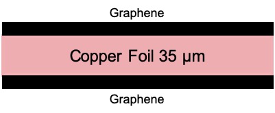
Graphene on Copper Foil (both sides)

Graphene on Copper Foil (Single-sided)
** Note: Copper Foil thickness is now 25μm now and if you need the old thickness of 45μm, please contact us for a quote.
**This product has a 1 year shelf life.
** Standard products have graphene on both sides of the copper foil.
** ACS Material can provide Single-sided CVD Graphene on Copper as shown in the drop-down list. It is prepared by depositing PMMA on the graphene, etch away the graphene on the back side and then remove PMMA. Please note that there might be minor PMMA residues on the graphene surface and you can do a deeper cleaner if necessary. Please contact us if you have any questions or have other special requests.
** ACS Material can also provide large size Monolayer CVD Graphene on Copper (Graphene Factory) made by CVD Method and large size Monolayer CVD Graphene on SiO2/Si by Metal Assisted Exfoliation (MAE Process). Order Now >>
3. Characterization & Analysis
Predominantly Single-layer Graphene on Copper Substrate
| Sheet Resistance | <600Ω/sq |
| Custom Order | <300Ω/sq |
| Transparency | >95% |
| Grain Size | ~50 μm |
.jpg)
Typical Raman Spectrum of a Single Layer Graphene
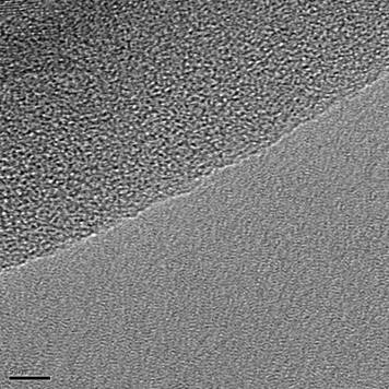
TEM Image of a Single Layer Graphene
Predominantly Double- or Multi-Layer Graphene.
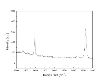
Typical Raman Spectrum of 2 Layers Graphene
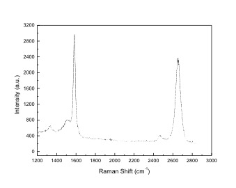
Typical Raman Spectra for 3-5 Layers Graphene
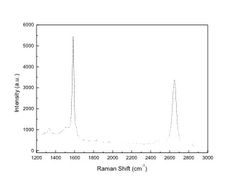
Typical Raman Spectra for 6-8 Layers Graphene
4. Conditions for safe storage
Keep the products in a dry and low oxygen (or oxygen-free) container at moderate temperature (<30°C).
*The shelf life of our CVD graphene on copper foil is 1 year.
5. ACS Material also provides:
- Super large size graphene on copper foil up to 30cmx20cm
- Double or multi-layer graphene
- Graphene transferred onto silicon dioxide substrate
- Pretreated graphene: Graphene has been coated PMMA‚ just after some simple steps‚ you can transfer it to other different substrates
- Customized service: different layers‚ different sizes of graphene; graphene transfer services etc.
Disclaimer: ACS Material LLC believes that the information on our website is accurate and represents the best and most current information available to us. ACS Material makes no representations or warranties either express or implied, regarding the suitability of the material for any purpose or the accuracy of the information listed here. Accordingly, ACS Material will not be responsible for damages resulting from use of or reliance upon this information.
FAQ
1. What's the difference between CVD graphene on copper foil and CVD graphene on copper foil (graphene factory)?
Our CVD Graphene on Copper Foil (Graphene Factory) product is designed for large size wafer transfers (up to 6x6in) and currently only the monolayer type is available. As the size increases there are likely to be more defects as compared to our standard CVD Graphene on Cu Foil. In general, our standard CVD Graphene on Copper Foil has better quality and the size is available up to 6inch x 4inch. This one has better monolayer graphene coverage because it is easier to control for smaller sizes. Both products are prepared by the CVD method, but we use a different set of equipment, so we name the products differently to make that distinction. You may choose whichever works best for your application.
2. What is the step by step transfer process of CVD graphene on copper foil onto my own substrates?
3. How much N-doped CVD graphene on copper foil would be?
4. What is the graphene layer thickness for each layers?
Research Citations of ACS Material Products
- Chen, Ruiyi, et al. “Co-Percolating Graphene-Wrapped Silver Nanowire Network for High Performance, Highly Stable, Transparent Conducting Electrodes.” Advanced Functional Materials, vol. 23, no. 41, 2013, pp. 5150–5158., doi:10.1002/adfm.201300124.
- O’Hern, Sean C., et al. “Selective Molecular Transport through Intrinsic Defects in a Single Layer of CVD Graphene.” ACS Nano, vol. 6, no. 11, Sept. 2012, pp. 10130–10138., doi:10.1021/nn303869m.
- Yoo, Jae-Hyuck, et al. “Graphene folds by femtosecond laser ablation.” Applied Physics Letters, vol. 100, no. 23, Apr. 2012, p. 233124., doi:10.1063/1.4724213.
- Longchamp, Jean-Nicolas, et al. “Low-Energy electron transmission imaging of clusters on free-Standing graphene.” Applied Physics Letters, vol. 101, no. 11, Oct. 2012, p. 113117., doi:10.1063/1.4752717.
- Chen, Xu-Dong, et al. “High-Quality and efficient transfer of large-Area graphene films onto different substrates.” Carbon, vol. 56, May 2013, pp. 271–278., doi:10.1016/j.carbon.2013.01.011.
- Ye, Qing., et al. “Polarization-Dependent optical absorption of graphene under total internal reflection.” Applied Physics Letters, vol. 102, no. 2, doi:10.1063/1.4776694.
- Longchamp, Jean-Nicolas, et al. “Ultraclean freestanding graphene by platinum-Metal catalysis.” Journal of Vacuum Science & Technology B, Nanotechnology and Microelectronics: Materials, Processing, Measurement, and Phenomena, vol. 31, no. 2, 2013, p. 020605., doi:10.1116/1.4793746.
- Wang, Yung Yu, and Peter J. Burke. “A large-Area and contamination-Free graphene transistor for liquid-Gated sensing applications.” Applied Physics Letters, vol. 103, no. 5, 2013, p. 052103., doi:10.1063/1.4816764.
- Wang, Peng, et al. “Accurate layers determination of graphene on transparent substrate based on polarization-Sensitive absorption effect.” Applied Physics Letters, vol. 103, no. 18, 2013, p. 181902., doi:10.1063/1.4827812.
- Zhou, Rong, et al. “Large-Energy, narrow-Bandwidth laser pulse at 1645 nm in a diode-Pumped Er:YAG solid-State laser passively Q-Switched by a monolayer graphene saturable absorber.” Applied Optics, vol. 53, no. 2, Sept. 2014, p. 254., doi:10.1364/ao.53.000254.
- Choi, Duyoung, et al. “Nanopatterned Graphene Field Effect Transistor Fabricated Using Block Co-Polymer Lithography.” Materials Research Letters, vol. 2, no. 3, Sept. 2014, pp. 131–139., doi:10.1080/21663831.2013.876676.
- Srisonphan, Siwapon, et al. “Space charge neutralization by electron-Transparent suspended graphene.” Scientific Reports, vol. 4, no. 1, 2014, doi:10.1038/srep03764.
- Joiner, C. A., et al. “Cleaning graphene with a titanium sacrificial layer.” Applied Physics Letters, vol. 104, no. 22, Feb. 2014, p. 223109., doi:10.1063/1.4881886.
- Roy, T., et al. “Tunneling characteristics in chemical vapor deposited graphene–hexagonal boron nitride–graphene junctions.” Applied Physics Letters, vol. 104, no. 12, 2014, p. 123506., doi:10.1063/1.4870073.
- Burke, Peter J. “Charging the Quantum Capacitance of Graphene with a Single Biological Ion Channel.” Biophysical Journal, vol. 106, no. 2, 2014, doi:10.1016/j.bpj.2013.11.2796.
- Li, Peining, et al. “Graphene-Enhanced Infrared Near-Field Microscopy.” Nano Letters, vol. 14, no. 8, 2014, pp. 4400–4405., doi:10.1021/nl501376a.
- Boutilier, Michael S. H., et al. “Implications of Permeation through Intrinsic Defects in Graphene on the Design of Defect-Tolerant Membranes for Gas Separation.” ACS Nano, vol. 8, no. 1, Mar. 2014, pp. 841–849., doi:10.1021/nn405537u.
- Lee, Jiye, et al. “Switching Individual Quantum Dot Emission through Electrically Controlling Resonant Energy Transfer to Graphene.” Nano Letters, vol. 14, no. 12, 2014, pp. 7115–7119., doi:10.1021/nl503587z.
- Srisonphan, Siwapon, and Komsan Hongesombut. “Tuning the ballistic electron transport of spatial graphene–metal sandwich electrode on a vacuum-Silicon-Based device.” RSC Advances, vol. 5, no. 3, 2015, pp. 2032–2037., doi:10.1039/c4ra09503k.
- Hui, Fei, et al. “Mechanical properties of locally oxidized graphene electrodes.” Archive of Applied Mechanics, vol. 85, no. 3, 2014, pp. 339–345., doi:10.1007/s00419-014-0957-4.
- Fujimoto, A, et al. “Negative magnetoresistance in Ti-Cleaned single-Layer graphene.” Journal of Physics: Conference Series, vol. 603, 2015, p. 012021., doi:10.1088/1742-6596/603/1/012021.
- Thareja, Vrinda, et al. “Electrically Tunable Coherent Optical Absorption in Graphene with Ion Gel.” Nano Letters, vol. 15, no. 3, 2015, pp. 1570–1576., doi:10.1021/nl503431d.
- Ye, X. H., et al. “Corrosion resistance of graphene directly and locally grown on bulk nickel substrate by laser irradiation.” RSC Advances, vol. 5, no. 45, 2015, pp. 35384–35390., doi:10.1039/c5ra01267h.
- Horvath, Cameron . “Fabrication and Characterization of Edge-Conformed Graphene-Silicon Waveguides.” IEEE Photonics Technology Letters, vol. 27, no. 6, 6 Jan. 2015, pp. 585–587., doi:10.1109/LPT.2014.2385757.
- Ye, Qing. “Polarization-Dependent optical absorption of graphene under total internal reflection.” Applied Physics Letters, vol. 102, no. 2, Jan. 2013, doi:10.1063/1.4776694.
- Zheng, Guanpeng, et al. “Improved Transfer Quality of CVD-Grown Graphene by Ultrasonic Processing of Target Substrates: Applications for Ultra-Fast Laser Photonics.” ACS Applied Materials & Interfaces, vol. 5, no. 20, Sept. 2013, pp. 10288–10293., doi:10.1021/am403205v.
- Zeng, Yong, et al. “Investigate the interface structure and growth mechanism of high quality ZnO films grown on multilayer graphene layers.” Applied Surface Science, vol. 301, 2014, pp. 391–395., doi:10.1016/j.apsusc.2014.02.088.
- Tang, Pinghua, et al. “Stable high-Energy Q-Switched resonantly diode-Pumped Er:YAG laser at 1645 nm.” OSA Publishing, vol. 53, no. 32, 2014, pp. 7773–7777., doi:10.1364/AO.53.007773.
- Watanabe, Hiroshi, et al. “Layer number dependence of carrier lifetime in graphenes observed using time-Resolved mid-Infrared luminescence.” Chemical Physics Letters, vol. 637, 2015, pp. 58–62., doi:10.1016/j.cplett.2015.07.046.
- He, Yingbo, et al. “Strongly enhanced Raman scattering of graphene by a single gold nanorod.” Applied Physics Letters, vol. 107, no. 5, Mar. 2015, p. 053104., doi:10.1063/1.4927759.
- Choi, Duyoung, et al. “Uniformly Nanopatterned Graphene Field-Effect Transistors with Enhanced Properties.” Nanoscale Research Letters, vol. 10, no. 1, Nov. 2015, doi:10.1186/s11671-015-0976-2.
- Miao, Lili, et al. “Broadband ultrafast nonlinear optical response of few-Layers graphene: toward the mid-Infrared regime.” Photonics Research, vol. 3, no. 5, 2015, p. 214., doi:10.1364/prj.3.000214.
- Hu, Jianchen, et al. “Improvement of the electrical contact resistance at rough interfaces using two dimensional materials.” Journal of Applied Physics, vol. 118, no. 21, July 2015, p. 215301., doi:10.1063/1.4936366.
- Jain, Tarun, et al. “Heterogeneous sub-Continuum ionic transport in statistically isolated graphene nanopores.” Nature Nanotechnology, vol. 10, no. 12, May 2015, pp. 1053–1057., doi:10.1038/nnano.2015.222.
- Srisonphan, Siwapon, and Komsan Hongesombut. “Tuning the ballistic electron transport of spatial graphene–metal sandwich electrode on a vacuum-Silicon-Based device.” RSC Advances, vol. 5, no. 3, 2015, pp. 2032–2037., doi:10.1039/c4ra09503k.
- Liu, Xiangjiang, et al. “Compact Shielding of Graphene Monolayer Leads to Extraordinary SERS-Active Substrate with Large-Area Uniformity and Long-Term Stability.” Scientific Reports, vol. 5, no. 1, 2015, doi:10.1038/srep17167.
- Hui, Fei, et al. “Moving graphene devices from lab to market: advanced graphene-Coated nanoprobes.” Nanoscale, vol. 8, no. 16, 2016, pp. 8466–8473., doi:10.1039/c5nr06235g.
- Ye, Xiaohui, et al. “Protecting carbon steel from corrosion by laser in situ grown graphene films.” Carbon, vol. 94, 2015, pp. 326–334., doi:10.1016/j.carbon.2015.06.080.
- Wu, Man, et al. “Wavelength switchable graphene Q-Switched fiber laser with cascaded fiber Bragg gratings.” Optics Communications, vol. 368, 2016, pp. 81–85., doi:10.1016/j.optcom.2016.01.069.
- Mackin, Charles, and Tomás Palacios. “Large-Scale sensor systems based on graphene electrolyte-Gated field-Effect transistors.” The Analyst, vol. 141, no. 9, 2016, pp. 2704–2711., doi:10.1039/c5an02328a.
- Politou, Maria, et al. “Multi-Layer graphene interconnect.” IEEE Xplore Digital Library , 11 July 2016, doi:10.1109/IITC-AMC.2016.7507731.
- Cao, Zhengmin, et al. “Nano-Gap between a gold tip and nanorod for polarization dependent surface enhanced Raman scattering.” Applied Physics Letters, vol. 109, no. 23, May 2016, p. 233103., doi:10.1063/1.4971832.
- Deng, Xiangquan, et al. “Terahertz-Induced photothermoelectric response in graphene-Metal contact structures.” Journal of Physics D: Applied Physics, vol. 49, no. 42, 2016, p. 425101., doi:10.1088/0022-3727/49/42/425101.
- Guo, Chu‐Cai, et al. “Experimental Demonstration of Total Absorption over 99% in the Near Infrared for Monolayer‐Graphene‐Based Subwavelength Structures.” Advanced Optical Materials, 1 Sept. 2016, onlinelibrary.wiley.com/doi/10.1002/adom.201600481/full.
- Hu, Jianbo, et al. “Rippling ultrafast dynamics of suspended 2D monolayers, graphene.” Proceedings of the National Academy of Sciences, vol. 113, no. 43, Oct. 2016, doi:10.1073/pnas.1613818113.
- Li, Cheng, et al. “Measurement of the Adhesion Energy of Pressurized Graphene Diaphragm Using Optical Fiber Fabry–Perot Interference.” IEEE Sensors Journal, vol. 16, no. 10, 2016, pp. 3664–3669., doi:10.1109/jsen.2016.2536783.
- Yuan, Jun, et al. “Modulation of far-Infrared light transmission by graphene-Silicon Schottky junction.” Optical Materials Express, vol. 6, no. 12, 2016, p. 3908., doi:10.1364/ome.6.003908.
- Li, Cheng, et al. “Measurement of thermal expansion coefficient of graphene diaphragm using optical fiber Fabry–Perot interference.” Measurement Science and Technology, vol. 27, no. 7, 2016, p. 075102., doi:10.1088/0957-0233/27/7/075102.
- Kafiah, Feras M., et al. “Monolayer graphene transfer onto polypropylene and polyvinylidenedifluoride microfiltration membranes for water desalination.” Desalination, vol. 388, 2016, pp. 29–37., doi:10.1016/j.desal.2016.02.027.
- Wu, Xiangyu. “Doping of graphene for the application in nano-Interconnect.” Microelectronic Engineering, vol. 167, 5 Jan. 2017, pp. 42–46., doi:10.1016/j.mee.2016.10.013.
- Liu, Siyang, et al. “Atomic emission spectroscopy of electrically triggered exploding nanoparticle analytes on graphene/SiO2/Si substrate.” Journal of Vacuum Science & Technology B, Nanotechnology and Microelectronics: Materials, Processing, Measurement, and Phenomena, vol. 34, no. 6, doi:10.1116/1.4964819.
- Sattler, Klaus D. Carbon nanomaterials sourcebook. Vol. 1, CRC Press, 2016.
- Politou, Maria. “Evaluation of multilayer graphene for advanced interconnects.” Microelectronic Engineering, vol. 167, 5 Jan. 2017, pp. 1–5., doi:10.1016/j.mee.2016.09.011.
- Hwang, Michael T., et al. “Highly specific SNP detection using 2D graphene electronics and DNA strand displacement.” Proceedings of the National Academy of Sciences, vol. 113, no. 26, 2016, pp. 7088–7093., doi:10.1073/pnas.1603753113.
- Nieto, Andy, et al. “Graphene reinforced metal and ceramic matrix composites: a review.” International Materials Reviews, vol. 62, no. 5, 2017, pp. 241–302., doi:10.1080/09506608.2016.1219481.
- Khorasaninejad, M., et al. “Highly Enhanced Raman Scattering of Graphene using Plasmonic Nano-Structure.” Scientific Reports, vol. 3, no. 1, 2013, doi:10.1038/srep02936.
- Kunz, Daniel A., et al. “Space-Resolved In-Plane Moduli of Graphene Oxide and Chemically Derived Graphene Applying a Simple Wrinkling Procedure (Adv. Mater. 9/2013).” Advanced Materials, vol. 25, no. 9, Apr. 2013, pp. 1336–1336., doi:10.1002/adma.201370060.
- Peng, Shuhua, et al. “Microwetting of Supported Graphene on Hydrophobic Surfaces Revealed by Polymerized Interfacial Femtodroplets.” Langmuir, vol. 30, no. 33, 2014, pp. 10043–10049., doi:10.1021/la5022774.
- Luo, Wen, et al. “Single-Layer Graphene as an Effective Mediator of the Metal–Support Interaction.” The Journal of Physical Chemistry Letters, vol. 5, no. 11, 2014, pp. 1837–1844., doi:10.1021/jz500425j.
- Suemoto, Tohru, et al. “Thickness dependent hot-Phonon effects observed by femtosecond mid-Infrared luminescence in graphene.” 19th International Conference on Ultrafast Phenomena, 2014, doi:10.1364/up.2014.07.mon.p1.32.
- Zhou, Haosen, et al. "Influence of CO2 On the Stability of Discharge Performance for Li-Air Battery with Hybrid Electrolyte Based On the Graphene Sheet”, Conference: 224th ECS Meeting. Oct. 2013, doi:10.1039/c3ra47258b.
- Thareja, Vrinda. “Electrically Tunable Optical Absorption in a Graphene-Based Salisbury Screen.” CORNELL UNIVERSITY LIBRARY, 7 Sept. 2014.
- Horvath, Cameron S. “Theses and Dissertations: Light Propagation and Photothermal Nonlinearity in Graphene-Si Waveguides.” University of Alberta Libraries, 26 Sept. 2013, doi:10.7939/R3ST1N .
- Li, Cheng, et al. “Interference characteristics in a Fabry–Perot cavity with graphene membrane for optical fiber pressure sensors.” Microsystem Technologies, vol. 21, no. 11, 2014, pp. 2297–2306., doi:10.1007/s00542-014-2333-2.
- Kou, Jun-Long, et al. “Platform for enhanced light–graphene interaction length and miniaturizing fiber stereo devices.” Optica, vol. 1, no. 5, 2014, p. 307., doi:10.1364/optica.1.000307.
- Karnik, Rohit. “Ionic and Molecular Transport Through Graphene Membranes.” Transport and Reactivity of Solutions in Confined Hydrosystems NATO Science for Peace and Security Series C: Environmental Security, Dec. 2013, pp. 95–102., doi:10.1007/978-94-007-7534-3_8.
- Warren, A.J, et al. “In vacuo X-Ray data collection from graphene-Wrapped protein crystals.” Acta Crystallographica Section D STRUCTURAL BIOLOGY, vol. 71, 1 Oct. 2015, pp. 2079–2088., doi:10.1107/S1399004715014194.
- Wen, Chenyu, et al. “Assessing kinetics of surface adsorption–desorption of gas molecules via electrical measurements.” Sensors and Actuators B: Chemical, vol. 223, 2016, pp. 791–798., doi:10.1016/j.snb.2015.10.019.
- Li, Cheng, et al. “Analyzing the applicability of miniature ultra-High sensitivity Fabry–Perot acoustic sensor using a nanothick graphene diaphragm.” Measurement Science and Technology, vol. 26, no. 8, Oct. 2015, p. 085101., doi:10.1088/0957-0233/26/8/085101.
- Li, Cheng, et al. “Analyzing the temperature sensitivity of Fabry-Perot sensor using multilayer graphene diaphragm.” OSA Publishing/ Optics Express, vol. 23, no. 21, 2015, pp. 27494–27502 ., doi:10.1364/OE.23.027494.
- Lau, K. Y., et al. “High Signal-To-Noise Ratio Q-Switching Erbium Doped Fiber Laser Pulse Emission Utilizing Single Layer Trivial Transfer Graphene Film Saturable Absorber.” Jurnal Teknologi, vol. 78, no. 3, 2016, doi:10.11113/jt.v78.7478.
- Zheng, Shijun, et al. “Acoustic charge transport induced by the surface acoustic wave in chemical doped graphene.” Applied Physics Letters, vol. 109, no. 18, 2016, p. 183110., doi:10.1063/1.4967192.
- Deng, Xiangquan, et al. “Terahertz-Induced photothermoelectric response in graphene-Metal contact structures.” Journal of Physics D: Applied Physics, vol. 49, no. 42, 2016, p. 425101., doi:10.1088/0022-3727/49/42/425101.
- Luo, Wen. “Graphene-Coated ZnO and SiO2 as Supports for CoO Nanoparticles with Enhanced Reducibility.” Chemphys, vol. 17, no. 19, 5 Oct. 2016, pp. 3055–3061., doi:10.1002/cphc.201600499.
- Lau, K.y., et al. “Passively mode-Locked soliton femtosecond pulses employing graphene saturable absorber.” Optics & Laser Technology, vol. 94, 2017, pp. 221–227., doi:10.1016/j.optlastec.2017.03.035.
- Fitri, Meika Aidil, et al. “Fabrication of TiO 2 -Graphene photocatalyst by direct chemical vapor deposition and its anti-Fouling property.” Materials Chemistry and Physics, vol. 198, 2017, pp. 42–48., doi:10.1016/j.matchemphys.2017.05.053.
- Li, Cheng, et al. “Nondestructive andin situdetermination of graphene layers using optical fiber Fabry–Perot interference.” Measurement Science and Technology, vol. 28, no. 2, Dec. 2017, p. 025206., doi:10.1088/1361-6501/aa54f8.
- Gao, Xiangyang, et al. “Measuring Graphene Adhesion on Silicon Substrate by Single and Dual Nanoparticle-Loaded Blister.” Advanced Materials Interfaces, vol. 4, no. 9, 2017, p. 1601023., doi:10.1002/admi.201601023.
- Tang, Xiaoduan, et al. “Five Orders of Magnitude Reduction in Energy Coupling across Corrugated Graphene/Substrate Interfaces.” ACS Applied Materials & Interfaces, vol. 6, no. 4, July 2014, pp. 2809–2818., doi:10.1021/am405388a.
- Morrow, W. K., et al. “(Invited) The Use of Graphene as a Solid State Diffusion Barrier.” ECS Transactions, vol. 61, no. 4, 2014, pp. 371–379., doi:10.1149/06104.0371ecst.
- Zheng, Haisheng, et al. “Ultrafine Pt nanoparticle induced doping/Strain of single layer graphene: experimental corroboration between conduction and Raman characteristics.” Journal of Materials Science: Materials in Electronics, vol. 26, no. 7, 2015, pp. 4746–4753., doi:10.1007/s10854-015-3043-y.
- Blinco , James P. “Spin-Coated carbon.” Chemical Science, no. 9, 12 June 2013, pp. 3411–3415., doi:10.1039/C3SC51396C.
- Zheng, H., et al. “Effect of Sub 1-Nm Pt Nanoparticle on the Conduction Properties of Graphene Based Field Effect Transistor.” ECS Transactions, vol. 61, no. 39, Jan. 2014, pp. 1–11., doi:10.1149/06139.0001ecst.
- Mckitterick, Christopher B., et al. “Electron-Phonon cooling in large monolayer graphene devices.” Physical Review B, vol. 93, no. 7, Apr. 2016, doi:10.1103/physrevb.93.075410
- Blinco , James P, et al. “Spin-Coated carbon.” Chemical Science, no. 9, 2013, pp. 3411–3415., doi:10.1039/C3SC51396C.
- Chan, Chun Yu. “Graphene based electrical biosensors for the detection of biomolecules.” The Hong Kong Polytechnic University, 2016.
- Pápa, Z., et al. “Spectroscopic ellipsometric investigation of graphene and thin carbon films from the point of view of depolarization effects.” Applied Surface Science, vol. 421, 2017, pp. 714–721., doi:10.1016/j.apsusc.2016.11.231.
- Hussain, Mushtaque, et al. “The improved piezoelectric properties of ZnO nanorods with oxygen plasma treatment on the single layer graphene coated polymer substrate.” Physica status solidi (a), vol. 211, no. 2, Oct. 2014, pp. 455–459., doi:10.1002/pssa.201300330.
- Kafiah, Feras, et al. “Synthesis of Graphene Based Membranes: Effect of Substrate Surface Properties on Monolayer Graphene Transfer.” Materials, vol. 10, no. 1, 2017, p. 86., doi:10.3390/ma10010086.
- Liang, Ji, et al. “Modulation of acousto-Electric current using a hybrid on-Chip AlN SAW/GFET device.” Applied Physics Letters, vol. 110, no. 24, Dec. 2017, p. 243504., doi:10.1063/1.4986481.
- Zhang, Yingjie, et al. "Electron transport in strain superlattices of graphene." Cornell University Library. 16 Mar. 2017.
- Yan, Xiao-Qing, et al. “Polarization dependence of graphene transient optical response: interplay between incident direction and anisotropic distribution of nonequilibrium carriers.” Journal of the Optical Society of America B, vol. 34, no. 1, 2016, p. 218., doi:10.1364/josab.34.000218.
- Lau, K.Y., et al. “Passively mode-Locked soliton femtosecond pulses employing graphene saturable absorber.” Optics & Laser Technology, vol. 94, 2017, pp. 221–227., doi:10.1016/j.optlastec.2017.03.035.
- Zhang, Yingjie, et al. “Electron transport in strain superlattices of graphene.” Research Gate, Mar. 2017.
- Peng, Shuhua, et al. “Microwetting of Supported Graphene on Hydrophobic Surfaces Revealed by Polymerized Interfacial Femtodroplets.” Langmuir, vol. 30, no. 33, 2014, pp. 10043–10049., doi:10.1021/la5022774.
- Horvath, Cameron, et al. “Edge-Conformed silicon-Graphene waveguides: Fabrication and measurements.” 11th International Conference on Group IV Photonics (GFP), 2014, doi:10.1109/group4.2014.6961953.
- Watanabe, Hiroshi, e al. “Femtosecond midi-Infrared luminescence with hot-Phonon effects in graphenes and graphite.”
- Hassan, Saad. Transparent conductive article.
- Liang, Ji, et al. “Manipulation of carriers in graphene using an on-Chip acoustic wave device.” 2017 IEEE International Ultrasonics Symposium (IUS), 2017, doi:10.1109/ultsym.2017.8092898.
- Luo, Wen, et al. “Interaction of bimetallic PtCo layers with bare and graphene-Covered ZnO(0001) supports.” Surface Science, vol. 669, 2018, pp. 64–70., doi:10.1016/j.susc.2017.11.001.
- Jiang, Wen-Shuai, et al. “Preparation of high-Quality graphene using triggered microwave reduction under an air atmosphere.” Journal of Materials Chemistry C, 2018, doi:10.1039/c7tc03957c.
- Dong, Nannan, et al. “Pressure and Temperature Sensor Based on Graphene Diaphragm and Fiber Bragg Gratings.” IEEE Photonics Technology Letters, 2017, pp. 1–1., doi:10.1109/lpt.2017.2786292.
- Huczko, Andrzej, et al. “Efficient one-Pot combustion synthesis of few-Layered graphene.” Physica status solidi (b), vol. 252, no. 11, 2015, pp. 2412–2417., doi:10.1002/pssb.201552233.
- Lu, Bingyu, et al. “Roughened cylindrical gold layer with curve graphene coating for enhanced sensitivity of fiber SPR sensor.” 2017 19th International Conference on Solid-State Sensors, Actuators and Microsystems (TRANSDUCERS), 2017, doi:10.1109/transducers.2017.7994461.
- Fitri, Meika Aidil, et al. “Fabrication of TiO 2 -Graphene photocatalyst by direct chemical vapor deposition and its anti-Fouling property.” Materials Chemistry and Physics, vol. 198, 2017, pp. 42–48., doi:10.1016/j.matchemphys.2017.05.053.
- Bezryadin, A, et al. “Large energy storage efficiency of the dielectric layer of graphene nanocapacitors.” Nanotechnology, vol. 28, no. 49, 2017, p. 495401., doi:10.1088/1361-6528/aa935c.
- Shi, Cheng, et al. “Metamaterial-Based graphene thermal emitter.” Nano Research, June 2017, doi:10.1007/s12274-017-1922-7.
- McCaffrey, Debra L., et al. “Mechanism of ion adsorption to aqueous interfaces: Graphene/Water vs. air/Water.” Proceedings of the National Academy of Sciences, vol. 114, no. 51, 2017, pp. 13369–13373., doi:10.1073/pnas.1702760114.
- Zhang, Qin, et al. “Negative differential resistance and hysteresis in graphene-Based organic light-Emitting devices.” Journal of Materials Chemistry C, The Royal Society of Chemistry, 1 Jan. 2018, pubs.rsc.org/en/Content/ArticleLanding/2017/TC/C7TC05148D#!
- Miskin, Marc Z., et al. “Graphene-Based bimorphs for micron-Sized, autonomous origami machines.” Proceedings of the National Academy of Sciences, vol. 115, no. 3, Feb. 2018, pp. 466–470., doi:10.1073/pnas.1712889115.
- Bukola, Saheed, et al. “Selective Proton/Deuteron Transport through Nafion|Graphene|Nafion Sandwich Structures at High Current Density.” Journal of the American Chemical Society, vol. 140, no. 5, 2018, pp. 1743–1752., doi:10.1021/jacs.7b10853.
- Brown, Morgan A., et al. “Graphene Biotransistor Interfaced with a Nitrifying Biofilm.” Environmental Science & Technology Letters, vol. 2, no. 4, Mar. 2015, pp. 118–122., doi:10.1021/acs.estlett.5b00025.
- Woo, Sung Oh, and Winfried Teizer. “The effect of electron induced hydrogenation of graphene on its electrical transport properties.” Applied Physics Letters, vol. 103, no. 4, 2013, p. 041603., doi:10.1063/1.4816475.
- Li, Cheng, et al. “Manipulation of Nonlinear Optical Properties of Graphene Bonded Fiber Devices by Thermally Engineering Fermi-Dirac Distribution.” Advanced Optical Materials, vol. 5, no. 21, 2017, doi:10.1002/adom.201770103.
- Chirayath, V. A, et al. “Positron induced electron emission from graphene.” IOP Science, Journal of Physics: Conference Series.
- Lock, Evgeniya H., et al. Stable IR Transparent Conductive Graphene Hybrid Materials and Methods of Making.
- Beechem, Thomas E., et al. “Self-Heating and Failure in Scalable Graphene Devices.” Scientific Reports, vol. 6, no. 1, Sept. 2016, doi:10.1038/srep26457.
- Ma, Yufeng, and Anni Siitonen. Chemical sensor using molecularly-Imprinted single layer graphene.
- Morrow, Wayne K., et al. “Role of graphene interlayers in mitigating degradation of Ni/Au ohmic contact morphology on p-Type GaN.” Vacuum, vol. 128, 2016, pp. 34–38., doi:10.1016/j.vacuum.2016.03.004.
- Nagamanasa, Kandula Hima, et al. “Liquid-Cell Electron Microscopy of Adsorbed Polymers.” Advanced Materials, vol. 29, no. 41, 2017, p. 1703555., doi:10.1002/adma.201703555.
- Hui, Fei. “Variability of graphene devices fabricated using graphene inks: Atomic force microscope tips.” Surface and Coatings Technology, vol. 320, 25 June 2017, doi:10.1016/j.surfcoat.2016.12.020.
- Chirayath, V A, et al. “Investigation of graphene using low energy positron annihilation induced Doppler broadening spectroscopy.” Journal of Physics: Conference Series, vol. 791, 2017, p. 012032., doi:10.1088/1742-6596/791/1/012032.
- Niu, Tianxiao, et al. “Indentation behavior of the stiffest membrane mounted on a very compliant substrate: Graphene on PDMS.” International Journal of Solids and Structures, vol. 132-133, 2018, pp. 1–8., doi:10.1016/j.ijsolstr.2017.05.038.
- Nashed, Ramy, et al. “Ultra-High Mobility in Dielectrically Pinned CVD Graphene.” IEEE Journal of the Electron Devices Society, vol. 4, no. 6, 2016, pp. 466–472., doi:10.1109/jeds.2016.2595498.
- Niu, Tianxiao, et al. “Fracture behavior of graphene mounted on stretchable substrate.” Carbon, vol. 109, 2016, pp. 852–859., doi:10.1016/j.carbon.2016.08.087.
- Boutilier, Michael S H, et al. “Knudsen effusion through polymer-Coated three-Layer porous graphene membranes.” Nanotechnology, vol. 28, no. 18, Oct. 2017, p. 184003., doi:10.1088/1361-6528/aa680f.
- Du, Feng, et al. “Surface stress of graphene layers supported on soft substrate.” Scientific Reports, vol. 6, no. 1, Nov. 2016, doi:10.1038/srep25653.
- Yokaribas, Volkan, et al. “Strain Gauges Based on CVD Graphene Layers and Exfoliated Graphene Nanoplatelets with Enhanced Reproducibility and Scalability for Large Quantities.” Sensors, vol. 17, no. 12, 2017, p. 2937., doi:10.3390/s17122937.
- Kuru, Cihan, et al. “Enhanced Power Conversion Efficiency of Graphene/Silicon Heterojunction Solar Cells Through NiO Induced Doping.” Journal of Nanoscience and Nanotechnology, vol. 16, no. 1, Jan. 2016, pp. 1190–1193., doi:10.1166/jnn.2016.12079.
- Korzeniewski, Carol, Jay P. Kitt, Saheed Bukola, Stephen E. Creager, Shelley D. Minteer, and Joel M. Harris. "Single Layer Graphene for Estimation of Axial Spatial Resolution in Confocal Raman Microscopy Depth Profiling." Analytical chemistry 91, no. 1 (2018): 1049-1055.
- Mackin, Charles E., and Tomás Apostol Palacios. "Sensor systems and related fabrication techniques." U.S. Patent Application 15/773,247, filed November 8, 2018.
- Wu, Ting, Abdullah Alharbi, Takashi Taniguchi, Kenji Watanabe, and Davood Shahrjerdi. "Low-frequency noise in irradiated graphene FETs." Applied Physics Letters 113, no. 19 (2018): 193502.
- Xie, Yadian. "Study on high-purity alumina preparation and its applications." PhD diss., Université du Québec à Chicoutimi, 2017.
- Liu, Siyang, Myungji Kim, and Hong Koo Kim. "Electrically-triggered micro-explosion in a graphene/SiO 2/Si structure." Scientific reports 8, no. 1 (2018): 7379.
- Ulibarri, Agatha. "Measuring the Double Layer Capacitance of Electrolyte Solutions Using a Graphene Field Effect Transistor." (2018).
- Das, Sonali, Mohammad Jobayer Hossain, Siu-Fung Leung, Anya Lenox, Yeonwoong Jung, Kristopher Davis, Jr-Hau He, and Tania Roy. "A leaf-inspired photon management scheme using optically tuned bilayer nanoparticles for ultra-thin and highly efficient photovoltaic devices." Nano Energy 58 (2019): 47-56.
- Laua, K. Y., A. A. Latifb, MH Abu Bakara, and M. A. Mahdia. "HIGH SIGNAL-TO-NOISE RATIO Q-SWITCHING ERBIUM DOPED FIBER LASER PULSE EMISSION UTILIZING SINGLE LAYER TRIVIAL TRANSFER GRAPHENE FILM SATURABLE ABSORBER." JURNAL TEKNOLOGI 78, no. 3 (2016): 129-133.
- Carmichael, Christopher P., M. Scott Smith, Arthur R. Weeks, and Donald C. Malocha. "Experimental Investigation of Surface Acoustic Wave Acoustoelectric Effect using a Graphene Film on Lithium Niobate." IEEE transactions on ultrasonics, ferroelectrics, and frequency control 65, no. 11 (2018): 2205-2207.
- Fujimoto, Akira, Christopher J. Perini, Daiju Terasawa, Akira Fukuda, Yoshiyuki Harada, Shigehiko Sasa, Mitsuaki Yano, and Eric M. Vogel. "Disorder and Weak Localization near Charge Neutral Point in Ti‐cleaned Single‐Layer Graphene." physica status solidi (b) (2019): 1800541.
- Zhao, Jingyi, Zhengmin Cao, Yuqing Cheng, Jianning Xu, Te Wen, Aiqin Hu, Qihuang Gong, and Guowei Lu. "In situ Optical Study of Gold Nanorod Coupling with Graphene." Advanced Optical Materials 6, no. 8 (2018): 1701043.
- Su, Fang, Zhaohao Zhang, Shasha Li, Peian Li, and Tao Deng. "Long-term stability of photodetectors based on graphene field-effect transistors encapsulated with Si3N4 layers." Applied Surface Science 459 (2018): 164-170.
- Ulibarri, Agatha. "Measuring the Double Layer Capacitance of Electrolyte Solutions Using a Graphene Field Effect Transistor." (2018).
- Dong, Nannan, Sumei Wang, Lan Jiang, Yi Jiang, Peng Wang, and Liuchao Zhang. "Pressure and temperature sensor based on graphene diaphragm and fiber Bragg gratings." IEEE Photonics Technology Letters 30, no. 5 (2018): 431-434.
- Lau, K. Y., MH Abu Bakar, AR Md Zain, A. F. Abas, M. T. Alresheedi, and M. A. Mahdi. "Stable multi-wavelength erbium-doped fiber laser assisted by graphene/PMMA thin film." Optics & Laser Technology 105 (2018): 129-134.
- Herekar, Satish. "Systems, methods, and kits to reduce surface heating during tissue treatment." U.S. Patent Application 15/896,886, filed June 28, 2018.
- Xu, Wendao, Lijuan Xie, Jianfei Zhu, Longhua Tang, Ranjan Singh, Chen Wang, Yungui Ma, Hou-Tong Chen, and Yibin Ying. "Terahertz biosensing with a graphene-metamaterial heterostructure platform." Carbon 141 (2019): 247-252.
- Deng, Tao, Zhaohao Zhang, Yaxuan Liu, Yingxin Wang, Fang Su, Shasha Li, Yang Zhang et al. "Three-dimensional graphene field-effect transistors as high-performance photodetectors." Nano letters (2019).
- Barnard, H. R., E. Zossimova, N. H. Mahlmeister, L. M. Lawton, I. J. Luxmoore, and G. R. Nash. "Boron nitride encapsulated graphene infrared emitters." Applied Physics Letters 108, no. 13 (2016): 131110.
- Wu, Xiangyu, Inge Asselberghs, Cedric Huyghebaert, Antonino Contino, Bart Soree, Marc Heyns, and Zsolt Tokei. "Graphene Interconnects-High Performance Twisted 20 nm Graphene Ribbons." In 2018 IEEE International Interconnect Technology Conference (IITC), pp. 25-27. IEEE, 2018.
- Li, Cheng, Xiyu Yu, Tian Lan, Jian Liu, and Shangchun Fan. "Insensitivity to Humidity in Fabry–Perot Sensor With Multilayer Graphene Diaphragm." IEEE Photonics Technology Letters 30, no. 6 (2018): 565-568.
- Dong, Nannan, and Bo Yang. "Simultaneous Measurement of Pressure and Temperature Based on Graphene." In IOP Conference Series: Materials Science and Engineering, vol. 382, no. 5, p. 052011. IOP Publishing, 2018.
- Zhang, Yingjie, Youngseok Kim, Matthew J. Gilbert, and Nadya Mason. "Electronic transport in a two-dimensional superlattice engineered via self-assembled nanostructures." npj 2D Materials and Applications 2, no. 1 (2018): 31.
- Mackin, Charles Edward. "Graphene chemical and biological sensors: modeling, systems, and applications." PhD diss., Massachusetts Institute of Technology, 2018.
- Yin, Yin, Jinbo Pang, Jiawei Wang, Xueyi Lu, Qi Hao, Ehsan Saei Ghareh Naz, Xinxing Zhou, Libo Ma, and Oliver G. Schmidt. "Graphene-Activated Optoplasmonic Nanomembrane Cavities for Photodegradation Detection." ACS applied materials & interfaces (2019).
- Andoy, Nesha M., Marcin S. Filipiak, Daniel Vetter, Óscar Gutiérrez‐Sanz, and Alexey Tarasov. "Graphene‐Based Electronic Immunosensor with Femtomolar Detection Limit in Whole Serum." Advanced Materials Technologies 3, no. 12 (2018): 1800186.
- Schweizer, Peter, Christian Dolle, and Erdmann Spiecker. "In situ manipulation and switching of dislocations in bilayer graphene." Science advances 4, no. 8 (2018): eaat4712.
- Hutzler, Andreas, Christian David Matthus, Christian Dolle, Mathias Rommel, Michael PM Jank, Erdmann Spiecker, and Lothar Frey. "Large-Area Layer Counting of Two-Dimensional Materials Evaluating the Wavelength Shift in Visible-Reflectance Spectroscopy." The Journal of Physical Chemistry C (2019).
- Hu, Ming, Yucong Yan, Kun Huang, Afzal Khan, Xiaodong Qiu, Dikai Xu, Hui Zhang, Xuegong Yu, and Deren Yang. "Performance Improvement of Graphene/Silicon Photodetectors Using High Work Function Metal Nanoparticles with Plasma Effect." Advanced Optical Materials 6, no. 9 (2018): 1701243.
- Hu, Shu-Kai, Fang-Yen Lo, Chih-Chen Hsieh, and Ling Chao. "Sensing Ability and Formation Criterion of Fluid Supported Lipid Bilayer Coated Graphene Field-Effect Transistors." ACS sensors (2019).
- Nemani, Srinivasa Kartik, Dayong Chen, Marwan H. Mohamed, and Hossein Sojoudi. "Stretchable and hydrophobic electrochromic devices using wrinkled graphene and PEDOT: PSS." Journal of Nanomaterials 2018 (2018).
- Wang, Kenan. "The Incorporation of Graphene to Lithium Cobalt Oxide as a Cathode to Improve the Performance of Lithium Ion Batteries." (2018).
- Cho, Hoduk. "The Use of Liquid Phase Transmission Electron Microscopy for Quantifying Interactions Between Colloidal Nanoparticles and Visualizing Their Self-Assembled Structures." PhD diss., UC Berkeley, 2018.
- Goldflam, Michael D., Isaac Ruiz, Stephen W. Howell, Joel R. Wendt, Michael B. Sinclair, David W. Peters, and Thomas E. Beechem. "Tunable dual-band graphene-based infrared reflectance filter." Optics express 26, no. 7 (2018): 8532-8541.
- Hutzler, A., C. D. Matthus, M. Rommel, and L. Frey. "Generalized approach to design multi-layer stacks for enhanced optical detectability of ultrathin layers." Applied Physics Letters 110, no. 2 (2017): 021909.

