
The thinnest material in the known world is graphene — a single sheet of carbon atoms locked in a honeycomb lattice that is just one atom thick, about 0.335 nanometers. That is roughly 300,000 times thinner than a typical sheet of printer paper, yet the sheet is strong enough to stand on its own and can even be seen with the naked eye. Graphene was first isolated as a stable, free-standing crystal in 2004, and its extraordinary thinness is the root of nearly every remarkable property it has.1
What is the thinnest thing in the world?
For everyday objects, “thin” means a fraction of a millimeter. Graphene operates in a completely different regime: its thickness is set by the size of a single carbon atom and the bonds that hold one sheet together. A monolayer of graphene is about 0.335 nm thick — the same as the spacing between the stacked carbon layers inside ordinary graphite, the “lead” in a pencil.2 Because a single layer cannot be made any thinner without ceasing to be a continuous solid, graphene represents a practical lower limit for the thickness of a stable material. This is why it is so often called the world’s thinnest material, and why it anchors a whole family of two-dimensional crystals. For the bigger picture of what graphene is and where it comes from, see our complete guide to graphene.
Subatomic particles and individual atoms are, of course, smaller still — but they are not materials you can pick up, layer, or build with. Among continuous, free-standing solids, a single atomic sheet is as thin as matter gets.
Why graphene is exactly one atom thick
Graphene is a crystalline allotrope of carbon. Each carbon atom forms three strong, in-plane covalent bonds to its neighbors through sp2 hybridization, producing a flat hexagonal mesh that looks like chicken wire. The carbon–carbon bond length is only about 0.142 nm, and because every atom sits in the same plane, the sheet has no “height” beyond a single atomic layer.2 The fourth electron on each carbon is delocalized above and below the plane, which gives graphene its conductivity but adds nothing to its thickness.
When many such sheets stack on top of one another, held together by weak van der Waals forces about 0.335 nm apart, the result is graphite. Pull off a single layer and you have graphene — the thinnest possible slice of that crystal. Measuring the mechanical behavior of one isolated sheet confirmed both its single-atom thinness and its astonishing strength.3
How thin is one atom, really?
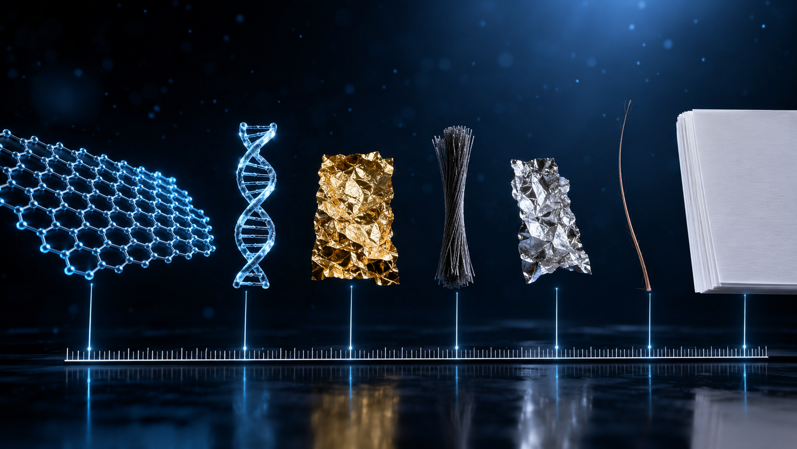
Numbers at the atomic scale are hard to picture, so it helps to compare graphene to things you can hold. The table below lists the approximate thickness of common thin objects and how many stacked graphene sheets it would take to match each one. The pattern is striking: you would need on the order of 300,000 layers of graphene just to equal a single sheet of printer paper.
| Object | Approximate thickness | Graphene layers to match | Note |
|---|---|---|---|
| Graphene (1 layer) | ~0.335 nm | 1 | The reference — one atom thick |
| DNA double helix (width) | ~2 nm | ~6 | A few atoms across |
| Thinnest gold leaf | ~100 nm | ~300 | Hand-beaten metal foil |
| Carbon fiber (single filament) | ~7 μm | ~21,000 | Often confused with graphene |
| Household aluminum foil | ~16 μm | ~48,000 | Everyday “thin” metal |
| Human hair | ~75 μm | ~224,000 | A common benchmark for “thin” |
| Sheet of printer paper | ~100 μm | ~299,000 | ~0.1 mm |
The interactive simulator below lets you stack graphene layers yourself and watch the total thickness climb on a logarithmic scale, with the hair and paper benchmarks marked for reference.
The takeaway from the model is the same one the table shows: a single graphene sheet sits at the very bottom of the thickness scale, and it takes an enormous number of layers — hundreds of thousands — before a graphene stack reaches the thickness of objects we casually call “thin.”
How do you even measure the thickness of one atom?
You cannot read a one-atom thickness with a ruler, so researchers use indirect methods. Transmission electron microscopy and electron diffraction can image a suspended sheet directly and count its layers; this is how the first free-standing single layers were confirmed.4 Atomic-force microscopy drags a sharp tip across a sheet resting on a substrate and reports a step height of a few angstroms (1 Å = 0.1 nm) where the graphene begins. A surprisingly elegant optical method also exists: because a single layer absorbs a fixed, measurable fraction of light, simply seeing the contrast of a flake on the right substrate reveals how many atomic layers are present.5 Capacitance and dielectric measurements give an “electrostatic” thickness of roughly 2.6 Å for a monolayer, consistent with the ~0.335 nm interlayer spacing seen in graphite.
Is graphene really two-dimensional?
A one-atom-thick crystal was long thought to be impossible. Classic statistical-mechanics arguments predicted that a strictly two-dimensional crystal would be thermodynamically unstable, with thermal vibrations destroying its long-range order at any finite temperature.6 Part of what made graphene’s isolation so significant was that it proved a stable two-dimensional atomic crystal could exist at room temperature.7
The resolution to the old paradox is that real graphene is not perfectly flat. Suspended sheets ripple gently in the third dimension, with nanoscale corrugations a fraction of a nanometer high.4 These intrinsic ripples are not a defect — they are exactly what stabilizes the sheet, allowing a genuinely one-atom-thick membrane to remain a coherent solid.8 Electronically, that thinness has dramatic consequences: charge carriers in graphene behave like massless relativistic particles, a direct result of its two-dimensional honeycomb structure.910
Why being one atom thick matters
Graphene’s thinness is not a curiosity for its own sake; nearly every headline property follows directly from having only one atomic layer:
- Nearly transparent. A single sheet absorbs only about 2.3% of visible light — a value set by fundamental constants rather than by any material parameter, precisely because the sheet is one atom thick.1112
- Almost weightless. One square meter of graphene weighs only about 0.77 milligrams — roughly 100,000 times lighter than the same area of typical office paper.
- Enormous surface area. With both faces of the sheet fully exposed, graphene offers a theoretical specific surface area near 2,630 m²/g — the whole material is surface, which is ideal for energy storage and sensing.13
- Outstanding heat and charge transport. An uninterrupted one-atom sheet conducts heat and electricity exceptionally well, with measured thermal conductivity among the highest of any material.14
- The thinnest possible barrier. Despite being one atom thick, a defect-free graphene membrane is impermeable even to helium, the smallest atom — effectively the world’s thinnest balloon.15 Stacked graphene-oxide membranes built from this material can let water through while blocking nearly everything else, the basis of graphene-based filtration.16
Taken together, these traits are why graphene is described not by any one superlative but by their combination — the thinnest, among the strongest, among the most conductive, and nearly transparent, all in one substance.17 As production methods mature, that combination is moving from the laboratory toward real products.18
Other ultrathin materials: the 2D family
Graphene opened the door to a whole library of atomically thin crystals. Once researchers saw that a single layer could be stable, they began isolating one-layer sheets of other materials, each thin enough to be considered two-dimensional.
- Molybdenum disulfide (MoS₂) — a single S–Mo–S layer is a direct-gap semiconductor, which (unlike graphene) gives it a natural band gap useful for transistors and light emission.1920
- Hexagonal boron nitride (hBN) — an atomically thin insulator, often used as an ultraflat, atomically smooth substrate that lets graphene perform at its best.21
- MXenes — two-dimensional metal carbides and nitrides, such as Ti₃C₂, produced by exfoliating a layered parent crystal; they are conductive and highly tunable.22
These sheets can even be stacked one atop another in a chosen sequence to build “van der Waals heterostructures” — designer materials assembled one atomic layer at a time.23 The breadth of this field, spanning graphene and related two-dimensional crystals, has been mapped out in detail by the research community.24 ACS Material supplies many of these materials through its graphene-like materials and MXene series product lines.
Thinnest, strongest, and lightest at once
It is easy to assume that the thinnest material must also be the most fragile. Graphene is the opposite. By indenting a free-standing single layer with an atomic-force microscope, researchers measured an intrinsic tensile strength of about 130 GPa and a stiffness near 1 TPa, establishing graphene as the strongest material ever measured.3 Compared like-for-like at the same thickness, that is on the order of a hundred times the strength of structural steel — the headline figures that depend on the sheet being defect-free and idealized. The remarkable point is that this strength and this extreme thinness coexist: a one-atom membrane that is also the toughest sheet known.
How is a one-atom-thick sheet made?
Producing something one atom thick takes specialized methods. The original approach was mechanical exfoliation — peeling single layers from graphite with adhesive tape.1 For larger areas, two routes dominate. Chemical vapor deposition (CVD) grows continuous single-layer films on a metal catalyst, enabling sheets large enough for electronics and transparent conductors.25 Epitaxial growth forms ultrathin graphitic layers on a silicon-carbide surface.26 A third family of methods produces graphene oxide in liquid, which can be processed into films and then reduced back toward conductive graphene — the basis of scalable, solution-based manufacturing.27 ACS Material offers research-grade CVD graphene, graphene oxide, and reduced graphene oxide for exactly these workflows.
What is the thinnest material used for?
Because so many useful properties flow from a single atomic layer, graphene and its ultrathin relatives are being applied across many fields:
- Transparent conductors for touch screens and flexible displays, where a near-invisible yet conductive film is needed — including roll-to-roll graphene films and hybrid graphene–silver-nanowire transparent conductive films.28
- Membranes and filtration that exploit graphene’s one-atom barrier to separate gases and purify water.16
- Ultra-sensitive sensors in which a molecule landing on the all-surface sheet produces a detectable change — sensitive enough to register a single gas molecule.29
- Energy storage — supercapacitor and battery electrodes that use graphene’s vast exposed area.13
- Composites in which a tiny mass of graphene reinforces or adds conductivity to a host material.30
Graphene and 2D materials from ACS Material
ACS Material manufactures and supplies graphene and related atomically thin materials for research and product development:
- Graphene Series — monolayer and few-layer graphene, the thinnest material in the catalog.
- CVD Graphene — continuous single-layer films on copper or transferred to your substrate.
- Graphene Oxide (GO) — solution-processable single sheets for films and membranes.
- Reduced Graphene Oxide (rGO) — conductive, restored graphene for electrodes and sensors.
- Graphene-like Materials — other 2D crystals including hBN and transition-metal dichalcogenides.
- MXene Series — conductive two-dimensional carbides such as Ti₃C₂.
Related reading
- Graphene Facts: Properties, Structure, Uses & Discovery — the complete pillar guide to graphene.
- Graphene vs. Graphite: What’s the Difference? — how a single one-atom layer differs from bulk, stacked graphite.
- Graphene and Its Application in Electronics — how thinness reshapes devices.
Frequently asked questions
What is the thinnest thing in the world?
The thinnest known material is graphene, a single sheet of carbon atoms about 0.335 nm thick — one atom thick. Individual atoms and subatomic particles are smaller, but they are not continuous, free-standing materials the way a graphene sheet is.
How thick is a single layer of graphene?
About 0.335 nanometers, the same as the spacing between carbon layers in graphite. The carbon–carbon bond within the sheet is about 0.142 nm long, and every atom lies in one plane.
Is graphene thinner than a human hair?
Yes — dramatically. A human hair is roughly 75,000 nm thick, so graphene is on the order of 200,000 times thinner. You would need hundreds of thousands of stacked graphene layers to match a single hair.
Is a human hair the thinnest fiber in the world?
No. Hair is often used as a benchmark for “thin,” but graphene is roughly 200,000 times thinner than a hair, and many engineered nanofibers are far thinner than hair as well.
If graphene is one atom thick, why can we see it?
Because a single layer absorbs about 2.3% of light — a small but visible amount. On the right background, that contrast is enough to make a one-atom-thick flake visible under an ordinary microscope, and sometimes to the naked eye.
Are there other one-atom-thick materials?
Yes. Graphene started a family of two-dimensional materials, including molybdenum disulfide (MoS₂), hexagonal boron nitride (hBN), and MXenes. Each is about one layer thick and has its own useful properties.
References
This article is provided by ACS Material LLC for educational purposes and describes graphene and related two-dimensional materials. Property values cited for an ideal single sheet — such as ~0.335 nm thickness, ~2.3% light absorption, ~2,630 m²/g surface area, ~130 GPa strength, and ~1 TPa stiffness — refer to idealized, defect-free, single-layer graphene and the specific studies referenced; multilayer material, films, or composites will differ, and actual performance depends on grade, number of layers, dispersion, and processing. Consult product datasheets and safety data sheets (SDS) for grade-specific specifications and handling guidance. The interactive simulator is a schematic teaching tool based on the stated layer-thickness model, not predictive design software.