-
Black Phosphorus | ACS Material
Jan 17, 2019 | ACS MATERIAL LLCA two-dimensional (2D) material similar to graphene, Black Phosphorus (BP) has many unique and noteworthy characteristics. The in-plane anisotropy deriving from its puckered orthorhombic structure affords extraordinary electronic, optical, transport, thermal and mechanical properties. Additionally, its high carrier mobility, tunability and moderate direct band gap makes BP a material of choice in electronics and optoelectronics. Furthermore, its biodegradability and biocompatibility makes BP suitable for applications in the biomedical field.14
Introduction
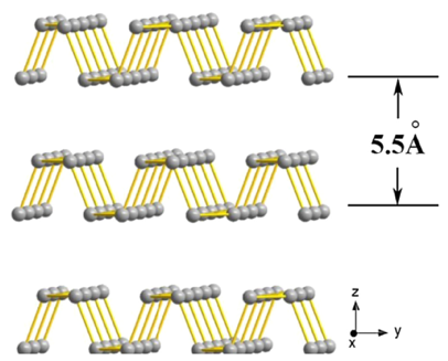
Phosphorus, an extraordinary element in group 5A of the periodic table, exists in different allotropic modifications, including white, black and amorphous red in ambient conditions.1 Among these allotropic forms, black phosphorus is the most stable, as first reported in 1914 by Bridgman.2-3 Orthorhombic Black Phosphorus (BP) is a layer-structured, high-mobility semiconductor, which gained great interest from both fundamental and applied science points of view. Each phosphorus atom is covalently bonded to three surrounding phosphorus atoms to form a pleated honeycomb structure in a monatomic layer (Figure 1).4-5

Figure 1. Schematic diagram of the microstructure of BP.9
Single or few-layer BP is also known as phosphorene and mimics the crystallographic characteristics of graphene, which is a two-dimensional layered material bonded by van der Waals forces between its layers.BP offers fascinating advantages over graphene and transition-metal dichalcogenides (TMDs) due to its unique in-plane anisotropy and high charge-carrier mobility.6-7 Compared with graphene, which has no band gap, BP has a direct band gap Eg that can be tuned from 0.3 to 2.0 eV by scaling down the layer thickness to a single layer.8-9Another significant advantage of BP is its relatively high charge carrier mobility of up to 1000 cm2/Vs observed from few-layer BP field-effect transistors (FETs) at room temperature. This value surpasses the mobility of TMDs-based FETs significantly.10It is reported that BP bridges the gap in the mobility/on-off ratio between graphene and TMD.11
For practical applications, BP is superior to TMDs due to its intrinsic ambipolar behavior, which is essential tothe construction of logic devices consisting of both n-and p-typesemiconductors.12
Despite its favorable characteristics, it is actually the environmental instability of BP that limits its applicability and further development. With its puckered honeycomb structure whereby one phosphorus atom is covalently bonded to three neighboringatoms, a lone pair of electrons is left exposed. These electrons readily react with oxygen and form PxOy in ambient conditions. The reaction between PxOy and water then results in the formation of phosphoric acid that leads tocompositional and physical change. Long-term exposure in air ultimately results in the etching away of the material. Several efforts have been reported with the purpose of improving the stability of BP in air.
Synthesis
Black phosphorus powders are synthesized by chemical vapor deposition (CVD) from red
phosphorus (99.999%) under a high temperature of 1000℃ and high pressure of 2 GPa for 10 minutes in a six-anvil cubic apparatus (Six WC anvils).Multi-layer BP nanosheets are prepared by a modified liquid exfoliation method from bulk BP. Ultrasound sonication with an ice bath of BP powder in isopropanol is used, followed by centrifugation to achieve ultrathin BP nanosheets with no sample contamination. Ultrasound probe sonication in N-methyl-2-pyrrolidone has the capability of producing large quantities of high-quality few-layered BP.
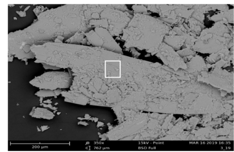
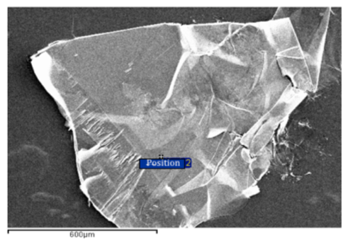
The SEM images of BP powders and crystals demonstrate a well-layered structure (Figure 2) as shown below.


Figure 2. Typical SEM Image of ACS Material Black Phosphorus
Powder (top) and Crystal (bottom).
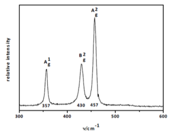
The Raman spectrum (Figure 3) shows the characteristic and phonons of few-layer black phosphorus.

Figure 3. Raman Spectrum Image of ACS Material Black Phosphorus.
Applications: Transistors
Transistors are the fundamental components in modern electronics and integrated circuits. BP exhibits excellent flexibility and also has unique advantages for 2D nanoelectronics. Two parameters of BP FETs, including mobility and on-off ratio, have been reported to be about 1000 cm2/Vs and 105 respectively at room temperature.18 These features are beneficial to the design and construction of transistors with low off-state power dissipation and high on-state power gain, which are crucial to the realization of high-speed logic circuits and high-frequency power amplifiers. Moreover, BP possesses ambipolar transport properties, which can facilitate the design of novel BP electronic devices.
Applications: Optoelectronic devices
Boasting thickness-dependent direct band gaps, spanning the visible to near-infrared (NIR) range and exhibiting large exciton binding energy and strong light-matter interaction, 2D BP is a great match for use in photodetectors and ultrafast pulse lasers. As an example, in 2014, Buscema et al. characterized the photo-response of ultrathin (3-8 nm) BP FETs showing optical responses from the visible region up to 940 nm with a cutoff wavelength of 997nm and rise time of 1 ms. The BP FETs also show good ability in mid-infrared photodetection in which the external responsivity could be as large as 82 A/W at 3.39 mm and is capable of performing low power detection in the picowatts range.20Wu et al. demonstrated the capability of BP in an ultraviolet (UV) photodetector with high responsivity and specific detectivity up to 9×10⁴ A/W and 3×10¹³, respectively.21 Furthermore, by employing BP flakes or BP quantum dots as the optical saturable absorber to turn the continuous wave output of the laser into a periodic train of optical pulses, the ultrafast pulse fiber lasers in the main telecommunication band 1.55 mm are produced.22
Applications: Battery anodes
BP has been a very promising anode material in Li-ion batteries even before extensive research on 2D BP crystals was done.23 Phosphorus is low-cost and abundant in nature. It can react with Li or Na to form Li3P or Na3P compounds with a high theoretical specific capacity of 2596 mAh/g at the discharge potential range of 0.4-1.2 V. Therefore, as the most stable allotrope of phosphorous, the crystalline and semiconducting BP is suitable for anode materials in batteries. For instance, Park et al. observed from conducting BP anodes high charging and discharging capacities of 2010 and 1814 mAh/g, respectively.24 However, the capacity faded rapidly due to the loss of electrical contact caused by the large volume expansion (300%) upon lithiation. To improve the cycling stability while accessing the full capacity, Sun et al. fabricated BP-graphite composites by high-energy mechanical milling to serve as anodes in Li-ion batteries.23 These composites deliver high capacity (2785 mAh/g) and excellent cycle life of 100 cycles with 80% capacity retention.
BP nanosheets are a good anode candidate in Na-ion batteries. By mixing the liquid dispersions of BP flakes and graphene, the BP-graphene composites serve as an anode in Na-ion batteries which show a high capacity of 2440 mAh/g and good cyclability with 83% capacity retention after 100 cycles.25 In addition to Li/Na ion batteries, nanoscale BP is suitable for electrode materials in solar cells. Yang et al. developed bifacial n-type dye-sensitized solar cells by incorporating BP quantum dots into a polyaniline film to serve as the photocathode.26
Applications: Phototherapy
With a thickness-dependent bandgap ranging from 0.3 to 2.0 eV, BP has broad absorption spanning from the UV to NIR regions of the energy spectrum and possesses interesting photophysical properties such as photothermal and photodynamic effects. Because of the high efficiency and minimal invasiveness, NIR-light induced photothermal therapy is currently undergoing fast development as an important supplement to traditional cancer therapy. The potential of BP as an antitumor photothermal therapy agent arises from its biocompatibility,
strong extinction coefficient and high photothermal conversion efficiency. Fu et al. investigated the photothermal efficiency of BP nanosheets with different sizes.29Compared with small BP quantum dots which possess good NIR photothermal efficiency, large BP nanosheets show higher efficiency in photothermal conversions.Conclusion
Phosphorus as a vital element has been studied for commercial applications such as fertilizers, feed additives, napalm bombs, and propellants. The emergence of 2D BP with fascinating properties has aroused extensive interests for applications in nanoelectronics, optoelectronics, energy, and biomedicine. Inspired by other types of 2D materials such as graphene and TMDs, there has been tremendous development with respect to BP. Future research and breakthroughs require the collaboration of scientists from different fields including material science, physics, chemistry, and biology.
ACS Material Products
References
1. S. Bocker and M. Haser, Z. Anorg. Allg. Chem. 321 (1995) 258.
2. A. Morita, Appl. Phys. A: Solid Surf. 39 (1986) 227-242.
3. Y. Akahama, S. Endo, and S. Narita, Physica B, 397 (1986) 139-140.
4. L. K. Li, G. J. Ye, Q. Ge, X. Ou, H. Wu, D. Feng, X. H. Chen, Y. Zhang, Nature Nanotech. 9 (2014) 372-377.
5. S. G. Peng, Y. Guo, G. X. Xie, J. B. Luo, Appl. Surf. Sci. 441 (2018) 670-677.
6. H. Liu, A. T. Neal, Z. Zhu, Z. Luo, X. Xu, D. Tomanek, and P. D. Ye, ACS Nano 8 (2014) 4033
7. A. K. Geim and S. K. Novoselov, Nat. Mater. 6 (2007) 183-191.
8. S. Das, W. Zhang, M. Demarteau, A. Hoffmann, M. Dubey, and A. Roelofs, Nano Lett. 14 (2014) 5733-5739.
9. J. Qiao, X. Kong, Z. X. Hu, F. Yang, and W. Ji, Nat. Commun. 5 (2014) 4475. 10. L. Li, Y. Yu, G.J. Ye, Q. Ge, X. Ou, H. Wu, D. Feng, Nat. Nanotechnol. 9 (2014) 372-377.
10. X. Ling, H. Wang, S. Huang, F. Xia, M.S. Dresselhaus, J. Lau, Proc. Natl. Acad. Sci. 112 (2015) 4523.
11. Y. Saito, Y. Iwasa, ACS Nano 9 (2015) 3192-3198.
12. Z. Luo, J. Maassen, Y. Deng, Y. Du, M.S. Lundstrom, P. D. Ye, X. Xu, Nat. Commun. 6 (2015) 8572.
13. Z. Sun, H. Xie, S. Tang, X.F. Yu, Z. Guo, J. Shao, H. Zhang, H. Huang, H. Wang, P.K. Chu, Angew. Chem. Int. Ed. 54 (2015) 11526-11530.
14. Q. Wei, J. He, Y S.ang, H. Jia, Y. Liu, W. Liu, Y. Liu, T. Li, Opt. Quant. Electron 48 (2016) 344.
15. A. Favron, E. Gaufres, F. Fossard, A. L. Phaneuf-L'Heureux, N. Y. Tang, P. L. Levesque, A. Loiseau, R. Leonelli, S. Francoeur, R. Martel, Nat. Mater. 14 (2015) 826-832.
16. D. Jariwala, V.K. Sangwan, L.J. Lauhon, T.J. Marks, M.C. Hersam, ACS Nano 8 (2014) 1102-1120.
17. L. Li, Y. Yu, G.J. Ye, Q. Ge, X. Ou, H. Wu, D. Feng, Nat. Nanotechnol. 9 (2014) 372-377.
18. M. Buscema, D.J. Groenendijk, S.I. Blanter, G.A. Steele, H.S.J. Van Der Zant, A. Castellanos-Gomez, Nano Lett. 14 (2014) 3347-3352.
19. Q. Guo, A. Pospischil, M. Bhuiyan, H. Jiang, H. Tian, D. Farmer, B. Deng, C. Li, S. J. Han, H. Wang, Q. Xia, T. P. Ma, T. Mueller, F. Xia, Nano Lett. 16 (2016) 4648-4655.
20. J. Wu, G.K.W. Koon, D. Xiang, C. Han, C.T. Toh, E.S. Kulkarni, I. Verzhbitskiy, A. Carvalho, A.S. Rodin, S.P. Koenig, G. Eda, W. Chen, A.H.C. Neto, B. Ozyilmaz, ACS Nano 9 (2015) 8070-8077.
21. Y. Chen, G. Jiang, S. Chen, Z. Guo, X. Yu, C. Zhao, H. Zhang, Q. Bao, S. Wen, D. Tang, D. Fan, Opt. Express 23 (2015) 12823-12833.
22. J. Sun, G. Zheng, H.W. Lee, N. Liu, H. Wang, H. Yao, W. Yang, Y. Cui, Nano Lett.14 (2014) 4573-4580.
23. C. M. Park, H. J. Sohn, Adv. Mater. 19 (2007) 2465-2468.
24. J. Sun, H. W. Lee, M. Pasta, H. Yuan, G. Zheng, Y. Sun, Y. Li, Y. Cui, Nat. Nanotechnol. 10 (2015) 980-985.
25. Y. Yang, J. Gao, Z. Zhang, S. Xiao, H. H. Xie, Z. B. Sun, J. H. Wang, C. H. Zhou, Y. W. Wang, X. Y. Guo, P. K. Chu, X. F. Yu, Adv. Mater. 28 (2016) 8937-8944.
26. Y. Chen, R. Ren, H. Pu, J. Chang, S. Mao, J. Chen, Biosens. Bioelectron. 89 (2017) 505-510.
27. V. Kumar, J. R. Brent, M. Shorie, H. Kaur, G. Chadha, A. G. Thomas, E. A. Lewis, A. P. Rooney, L. Nguyen, X. L. Zhong, M.G. Burke, S. J. Haigh, A. Walton, P. D. McNaughter, A. A. Tedstone, N. Savjani, C. A. Muryn, P. O’Brien, A. K. Ganguli, D. J. Lewis, P. Sabherwal, ACS Appl. Mater. Interfaces 8 (2016) 22860-22868.
28. H. D. Fu, Z. B. Li, H. H. Xie, Z. B. Sun, B. K. Wang, H. Huang, G. L. Han, H. Y. Wang, P. K. Chu, X. F. Yu, RSC Adv. 7 (2017) 14618-14624.